linux-chenxing.org
ISP
The chips have two i2c slaves behind the uart pins that seems to work even when the uart is on.
For example on a mercury5 device with the uart pins connected to the i2c controller of a board running linux we can see two slaves on the bus:
$ i2cdetect -y 0
     0  1  2  3  4  5  6  7  8  9  a  b  c  d  e  f
00:          -- -- -- -- -- -- -- -- -- -- -- -- --
10: -- -- -- -- -- -- -- -- -- -- -- -- -- -- -- --
20: -- -- -- -- -- -- -- -- -- -- -- -- -- -- -- --
30: -- -- -- -- -- -- -- -- -- -- -- -- -- -- -- --
40: -- -- -- -- -- -- -- -- -- 49 -- -- -- -- -- --
50: -- -- -- -- -- -- -- -- -- 59 -- -- -- -- -- --
60: -- -- -- -- -- -- -- -- -- -- -- -- -- -- -- --
70: -- -- -- -- -- -- -- --
These i2c slaves are present on infinity, infinity3, infinity2m, pioneer3.. and probably everything else.
Disabling PM_UART RX for easier access to ISP
Clear the PM_UART rx enable bit
mw.w 0x1f001c24 0x0
Debug tool
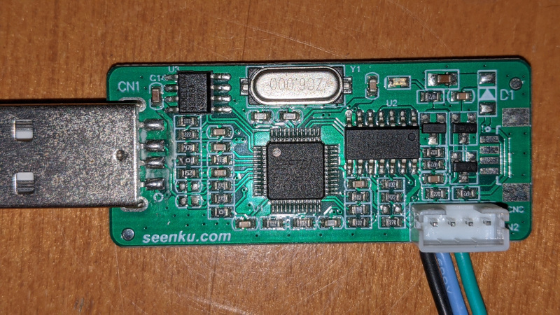
- FTDI FT2232D
- NXP 74HC08D (Quad 2-input AND gate)
- Atmel 93C56A (2Kb EEPROM)
Homebrew
- Adafruit 5v trinket.
- flashrom - If you have SPI NOR flash.
- If configured correctly flashrom has a driver that can talk via i2c to the flash very slowly.
make CONFIG_MSTARDDC_SPI=yes./flashrom -p mstarddc_spi:dev=/dev/i2c-1:0x49
- SNANDer fork with mstarddc support - If you have SPI NAND flash, can be also used for SPI NOR.
- Same deal as flashrom, very slow!
- Good enough to write the required blobs and u-boot.
./SNANDer -p mstarddc -c /dev/i2c-4:49 -i
General stuff
Interface activation
By default (after reset or an exit command), these interfaces are deactivated, and in order to activate them, a special synchronization string should be sent as a single transfer.
- For ISP: “MSTAR” (0x4D 0x53 0x54 0x41 0x52)
- For SERDB: “SERDB” (0x53 0x45 0x52 0x44 0x42)
Command protocol
The protocol is command-based, and basically it looks like this:
- Each command starts with an write transfer to (obviously) send a command byte.
- If the command has some arguments/tx data, then it follows the command byte in the same transfer.
- If the command has some response/rx data, then it is received with an read transfer.
It’s that simple.
ISP interface
The ISP (In-System Programmer) interface exposes the SPI bus which is used by the onboard SPI flash (the one that is on the PM_SPI_xxx pins).
It lives on these I2C addresses:
- 0x49
- 0x51 on MSB123xC
Commands
- 0x10: Send data over SPI
- 0x11: Receive data from SPI
- 0x12: End SPI transaction (pull up CS)
- 0x20: Read status? 0xC0 when idle, 0x80 when communication ongoing.
- 0x21: ? Resets the CRC register to 0xffff and on some chips breaks SPI
- 0x22: Read CRC register bits 8..15
- 0x23: Read CRC register bits 0..7
- 0x24: Exit ISP / Reset
- 0x25: ? The ISP slave disappears, SPI bus is inaccessible, and on MSB123xC the SDA line pulls down permanently.
The CRC register
It uses the polynomial 0x8005 (x16 + x15 + x2 + 1), and it is somewhat weird.
It updates only when data is transferred out of the SPI bus (by using 0x10 command), and the value which it uses to calculate it goes from weird internal state register.
That internal state register can be accessed by reading past the length that the command returns (e.g. for 0x20/0x22/0x23 it’s 1 byte, for 0x21 it’s 0 bytes)
The value it has is either a “next” byte that is going to be received on SPI, or a last byte that has been sent over SPI (not the byte you sent that triggered this exact CRC update!)
Just look at that:
00000000: 27 05 19 56 8e 8c c5 81 61 b9 fe 38 00 04 f7 22  |'..V....a..8..."|
00000010: 87 5f 01 80 87 5f 06 00 7b 13 27 d5 11 05 02 03  |._..._..{.'.....|
00000020: 4d 53 74 61 72 20 4d 53 44 37 38 31 36 20 55 2d  |MStar MSD7816 U-|
00000030: 42 6f 6f 74 00 00 00 00 00 00 00 00 00 00 00 00  |Boot............|
00000040: 5d 00 00 80 00 ff ff ff ff ff ff ff ff 00 00 1b  |]...............|
00000050: 04 55 3f d3 d1 56 64 2c 9c 6d 7b 38 a6 21 71 4a  |.U?..Vd,.m{8.!qJ|
00000060: 6e 20 ea 3a -- -- -- -- -- -- -- -- -- -- -- --  |n .:            |
                   ^^
              the last byte there is 0x3a
(system resets there, previous read has no effect there)
ff:ff <- rst
fd:02 <- sent 0x03 but it did 0x00
80:07 <- sent 0x01 but it did 0x03
04:06 <- sent 0x00 but it did 0x01
86:1b <- sent 0x00 and it did 0x00
00000000: 27 05 19 56 8e 8c c5 81 61 b9 fe 38 00 04 f7 22  |'..V....a..8..."|
00000010: 87 5f 01 80 87 5f 06 00 7b 13 27 d5 11 05 02 03  |._..._..{.'.....|
00000020: 4d 53 74 61 72 20 4d 53 44 37 38 31 36 20 55 2d  |MStar MSD7816 U-|
00000030: 42 6f 6f 74 00 00 00 00 00 00 00 00 00 00 00 00  |Boot............|
00000040: 5d 00 00 80 00 ff ff ff ff ff ff ff ff 00 00 1b  |]...............|
00000050: 04 55 3f d3 d1 56 64 2c 9c 6d 7b 38 a6 21 71 4a  |.U?..Vd,.m{8.!qJ|
00000060: 6e 20 ea -- -- -- -- -- -- -- -- -- -- -- -- --  |n .             |
                ^^ ^^
           there we read one byte less, the following byte is 0x3a
86:1b <- read does not affect it at all
98:8b <- sent 0x03 but it did 0x3a (the byte we didn't read yet!)
08:59 <- same as before
59:36 <- same...
37:d6 <- sent 0x01 but it did 0x00
37:d6 <- we didnt read there
======= <- there is the cmd 0x21
ff:ff <- crc reset
7d:07 <- sent 0x03 but it did 0x01 (the last byte i sent previously!)
06:04
84:11
12:18
00000000: ff ff ff ff ff ff ff ff ff ff ff ff ff ff ff ff  |................|
00000010: ff ff ff ff ff ff ff ff ff ff ff ff ff ff ff ff  |................|
00000020: ff ff ff ff ff ff ff ff ff ff ff ff ff ff ff ff  |................|
00000030: ff ff ff ff ff ff ff ff ff ff ff ff ff ff ff ff  |................|
00000040: ff ff ff ff ff ff ff ff ff ff ff ff ff ff ff ff  |................|
00000050: ff ff ff ff ff ff ff ff ff ff ff ff ff ff ff ff  |................|
00000060: ff ff ff ff -- -- -- -- -- -- -- -- -- -- -- --  |....            |
           ^^^^^^^
      cmd 0x21 broke the SPI bus somehow, and now everything reads out as 0xff
12:18 <- nothing changed as well
SERDB interface
The SERDB (SERial DeBug) interface basically exposes internal chip busses (mainly RIU), as well as some other misc control for doing some kind of debugging or e.g. bringing up a chip.
It lives on these I2C addresses:
- 0x59
- 0x5A on Kronus
- 0x62 on MSG2138
- 0x69 on MSB123xC
Commands
- 0x10: Bus access
- Starts with 2 or 4 bytes of address to be accessed, big endian.
- 0x34: Disable bus access
- 0x35: Enable bus access
- 0x36: Resume MCU
- 0x37: Stop MCU
- 0x45: Exit SERDB (note: this is NAKed!)
- 0x51: ? sent when it’s about to stop MCU, next cmd is 0x35
- 0x53: ? sent when it’s not about to stop MCU, next cmd is 0x7F
- 0x61: ?
- 0x70: ?
- 0x71: “i2c reshape”
- 0x80: Channel no. bit 0 clear
- 0x81: Channel no. bit 0 set
- 0x82: Channel no. bit 1 clear
- 0x83: Channel no. bit 1 set
- 0x84: Channel no. bit 2 clear
- 0x85: Channel no. bit 2 set
Variants
The “older” one
This variant uses 16 bit bus addressing, and accesses only the 8051 XDATA bus (since MStar was making 8051-based chips at that time).
In SoCs where the PM and Non-PM parts were split, the address 0x0000 now is used to store the address bits 16..23.
For example, to access 0x101FFE, you write 0x10 to 0x0000, then access 0x1FFE. To access 0x110C32, write 0x11 to 0x0000, then access 0x0C32. And to access 0x001ECC, write 0x00 to 0x0000, then access 0x1ECC.
It’s that simple.
The “newer” one
This variant uses 32 bit bus addressing, and introduced bus channel switching, which also introducted direct access to both parts of RIU (PM and Non-PM), thus making the 8051 XDATA mapping useful mostly in accessing DRAM via XDMIU.
However, it seems like there is also an intermediate variant where the addressing is still 16 bit but it does have channel switching and all the stuff the newer variant has… clues … yes, this is basically mstarddc_spi but with hardcoded i2c addresses and it also uses SERDB to control the WP pin…
The bus channels is listed below:
| ch | Bus |
|---|---|
| 0 | 8051 XDATA |
| 1 | |
| 2 | |
| 3 | PM RIU |
| 4 | Non-PM RIU |
| 5 | |
| 6 | |
| 7 |
ISP SPI protocol
Some details on the SPI over i2c protocol are here. The same windows tool is used for all MStar chips it seems so this is probably valid across the board.
The 0x49 i2c slave is the SPI bridge to the flash.
ISP DEBUG protocol
- Lives on the 0x59 slave
- synchronization string is “SERDB”.
Reading a bank of registers looks like this:
Writing "SERDB"

i2c-1: Write
i2c-1: Address write: B2
i2c-1: Data write: 53
i2c-1: Data write: 45
i2c-1: Data write: 52
i2c-1: Data write: 44
i2c-1: Data write: 42
---
Setting up something? Memory dump also has this sequence

i2c-1: Write
i2c-1: Address write: B2
i2c-1: Data write: 81
i2c-1: Write
i2c-1: Address write: B2
i2c-1: Data write: 83
i2c-1: Write
i2c-1: Address write: B2
i2c-1: Data write: 84
i2c-1: Write
i2c-1: Address write: B2
i2c-1: Data write: 53
i2c-1: Write
i2c-1: Address write: B2
i2c-1: Data write: 7F
i2c-1: Write
i2c-1: Address write: B2
i2c-1: Data write: 35
i2c-1: Write
i2c-1: Address write: B2
i2c-1: Data write: 71
i2c-1: Write
i2c-1: Address write: B2
i2c-1: Data write: 34
i2c-1: Write
i2c-1: Address write: B2
i2c-1: Data write: 45
---
"SERDB" again

i2c-1: Write
i2c-1: Address write: B2
i2c-1: Data write: 53
i2c-1: Data write: 45
i2c-1: Data write: 52
i2c-1: Data write: 44
i2c-1: Data write: 42

---
Another common senquence between register dump and mem dump

i2c-1: Write
i2c-1: Address write: B2
i2c-1: Data write: 81
i2c-1: Write
i2c-1: Address write: B2
i2c-1: Data write: 83
i2c-1: Write
i2c-1: Address write: B2
i2c-1: Data write: 84
i2c-1: Write
i2c-1: Address write: B2
i2c-1: Data write: 53
i2c-1: Write
i2c-1: Address write: B2
i2c-1: Data write: 7F
i2c-1: Write
i2c-1: Address write: B2
i2c-1: Data write: 35
i2c-1: Write
i2c-1: Address write: B2
i2c-1: Data write: 71
i2c-1: Write
---
Common between reg dump and memdump

i2c-1: Address write: B2
i2c-1: Data write: 10
i2c-1: Data write: 00
i2c-1: Data write: 00
i2c-1: Data write: 1E
i2c-1: Data write: CF
i2c-1: Read
---
Common

i2c-1: Address read: B3
i2c-1: Data read: 00
i2c-1: Write
---
Common
i2c-1: Address write: B2
i2c-1: Data write: 10
i2c-1: Data write: 00
i2c-1: Data write: 00
i2c-1: Data write: 1E
i2c-1: Data write: CC
i2c-1: Read
---
common
i2c-1: Address read: B3
i2c-1: Data read: F5
i2c-1: Write
---
common
i2c-1: Address write: B2
i2c-1: Data write: 10
i2c-1: Data write: 00
i2c-1: Data write: 00
i2c-1: Data write: 1E
i2c-1: Data write: CD
i2c-1: Read
---
common
i2c-1: Address read: B3
i2c-1: Data read: 00
i2c-1: Write
---
common
i2c-1: Address write: B2
i2c-1: Data write: 34
i2c-1: Write
---
common
i2c-1: Address write: B2
i2c-1: Data write: 45
i2c-1: Write
---
common
i2c-1: Address write: B2
i2c-1: Data write: 53
i2c-1: Data write: 45
i2c-1: Data write: 52
i2c-1: Data write: 44
i2c-1: Data write: 42
i2c-1: Write
---
common
i2c-1: Address write: B2
i2c-1: Data write: 81
i2c-1: Write
---
common
i2c-1: Address write: B2
i2c-1: Data write: 83
i2c-1: Write
---
common
i2c-1: Address write: B2
i2c-1: Data write: 84
i2c-1: Write
---
common
i2c-1: Address write: B2
i2c-1: Data write: 53
i2c-1: Write
---
common
i2c-1: Address write: B2
i2c-1: Data write: 7F
i2c-1: Write
---
common
i2c-1: Address write: B2
i2c-1: Data write: 35
i2c-1: Write
---
common
i2c-1: Address write: B2
i2c-1: Data write: 71
i2c-1: Write
---
*** reg dump and mem dump diverge here ***
---
"SERDB"
i2c-1: Address write: B2
i2c-1: Data write: 53
i2c-1: Data write: 45
i2c-1: Data write: 52
i2c-1: Data write: 44
i2c-1: Data write: 42
i2c-1: Write
---
i2c-1: Address write: B2
i2c-1: Data write: 81
i2c-1: Write
i2c-1: Address write: B2
i2c-1: Data write: 83
i2c-1: Write
i2c-1: Address write: B2
i2c-1: Data write: 84
i2c-1: Write
i2c-1: Address write: B2
i2c-1: Data write: 53
i2c-1: Write
i2c-1: Address write: B2
i2c-1: Data write: 7F
i2c-1: Write
i2c-1: Address write: B2
i2c-1: Data write: 35
i2c-1: Write
i2c-1: Address write: B2
i2c-1: Data write: 71
i2c-1: Write
---

This looks like a command and then bank 0x30?

i2c-1: Address write: B2
i2c-1: Data write: 10
i2c-1: Data write: 00
i2c-1: Data write: 00
i2c-1: Data write: 30
i2c-1: Data write: 00
i2c-1: Read
---

Register values?

i2c-1: Address read: B3
i2c-1: Data read: 00
i2c-1: Data read: 00
i2c-1: Data read: 00
i2c-1: Data read: 00
i2c-1: Data read: 00
i2c-1: Data read: 09
i2c-1: Data read: FF
i2c-1: Data read: FF
Channel select
A lot of the above seems to be the sequence to select the desired channel
- Channel select sequence:
- https://github.com/jockyw2001/utopia/blob/53ee8cc121a030b8d368113ac3e966b4705770ef/UTPA2-700.0.x/modules/demodulator/hal/maldives/demod/halDMD_INTERN_common.c#L319
Booting from SDRAM
https://github.com/fifteenhex/SDK_pulbic/blob/c1436fa7446457e8d6547874d27ee4e34be150cf/Mercury5/proj/sc/driver/hal/mercury/kernel/inc/kernel_chiptop.h#L1897
ISP tool scripts
- swch - Switch channel?
- 0 - DRAM?
- 3 - PM registers
- 4 - Normal registers
- wsdr - Write a file?
- wriu - Write a register
-bwrite a byte?-wwrite a word?
- wait - Wait for N seconds?
Command bytes
- 0x10 - Seems to be set address
- 0x34 - Seems to be exit from something
- 0x80 - Clear channel bit 0
- 0x81 - Set channel bit 0
- 0x82 - Clear channel bit 1
- 0x83 - Set channel bit 1
- 0x84 - Clear channel bit 2
- 0x85 - Set channel bit 2
0x51 0x53 0x37 0x7F 0x35 0x71